- 您现在的位置:买卖IC网 > Sheet目录341 > MAX8821ETI+ (Maxim Integrated)IC LED DRVR WHITE BCKLGT 28-TQFN
�� �
�
�White� LED� Charge� Pump� with� Mono� Class� D�
�Audio� Amp� and� Dual� LDO�
�Table� 16.� PUMP_CNTL� (Address� 0x0E)�
�Applications� Information�
�BIT�
�B7–B3�
�B2�
�NAME�
�N/A,� do� not� use�
�TEMP_DR�
�CODE�
�0�
�1�
�DESCRIPTION�
�Temperature�
�derating� disabled.�
�Temperature� derating�
�enabled.�
�PCB� Layout�
�PCB� layout� is� essential� for� optimizing� performance.� Use�
�large� traces� for� the� power-supply� inputs� and� amplifier�
�outputs� to� minimize� losses� due� to� parasitic� trace� resis-�
�tance� and� to� route� heat� away� from� the� device.� To� avoid�
�potential� noise� to� the� differential� input� audio� signal� and�
�differential� output� audio� signal,� route� the� negative� and�
�Charge� pump�
�positive� traces� in� parallel.� Also,� avoid� placing� any� RF� or�
�00�
�automatically�
�changes� between�
�high-speed� data� signals� in� parallel� to� the� audio� signals.�
�In� some� applications,� such� as� GSM,� extra� noise� reduc-�
�B1,� B0�
�PUMP_CNTL� [1:0]�
�01�
�10�
�1x/1.5x� mode.�
�Charge� pump� is�
�forced� into� 1.5x� mode�
�regardless� of� input�
�voltage.�
�Charge� pump� is�
�forced� into� 1.5x� mode�
�regardless� of� input�
�voltage� when� audio�
�amplifier� is� enabled.� If�
�the� amplifier� is� not�
�enabled,� the� charge�
�tion� may� be� needed.� To� reduce� the� risk� of� noise,� place�
�16pF� ceramic� capacitors� from� AIN+� to� AGND,� AIN-� to�
�AGND,� OUT+� to� AGND,� OUT-� to� AGND,� OUT+� to� OUT-,�
�and� AIN+� to� AIN-.�
�Proper� grounding� improves� audio� performance� and�
�prevents� any� digital� switching� noise� from� coupling� into�
�the� audio� signal.� The� Thin� QFN� package� features� an�
�exposed� thermal� paddle� on� its� undersides.� This� paddle�
�lowers� the� thermal� resistance� of� the� package� by� provid-�
�ing� a� direct-heat� conduction� path� from� the� die� to� the�
�PCB.� Connect� the� exposed� paddle� to� AGND� directly�
�under� the� IC.� Refer� to� the� MAX8821� Evaluation� Kit� for�
�pump� automatically�
�switches� between� 1x�
�mode and 1.5x mode.�
�an� example� of� a� PCB� layout.�
�Note:� Defaults� in� bold� italics.�
�11�
�N/A,� do� not� use.�
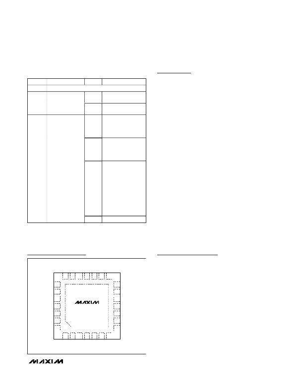
�TOP� VIEW�
�Pin� Configuration�
�PROCESS:� BiCMOS�
�Chip� Information�
�21�
�20�
�19�
�18�
�17�
�16�
�15�
�C2N� 22�
�C1N� 23�
�C2P� 24�
�14�
�13�
�12�
�REF�
�AGND�
�SDA�
�C1P� 25�
�IN1� 26�
�PGND1� 27�
�MAX8821ETI+�
�11�
�10�
�9�
�SCL�
�LDO1�
�LDO2�
�EP� =� EXPOSED� PADDLE�
�IN3� 28�
�8�
�IN2�
�+�
�1�
�2�
�3�
�4�
�5�
�6�
�7�
�______________________________________________________________________________________�
�27�
�发布紧急采购,3分钟左右您将得到回复。
相关PDF资料
MAX8822ETE+T
IC LED DRVR WHITE BCKLGT 16-TQFN
MAX8830EWE+T
IC LED DRVR WHITE BCKLGT 16-UCSP
MAX8831EWE+T
IC LED DRIVR WHITE BCKLGT 16-WLP
MAX8834ZEWP+T
IC LED DRIVR BCKLGT FLASH 20-WLP
MAX8855EVKIT+
KIT EVAL FOR MAX8855
MAX8879ETG+T
IC LED DRVR WT/RGB BCKLGT 24TQFN
MAX8901BETA+TCH8
IC LED DRIVER WHITE BCKLGT 8TDFN
MAX8930EWJ+T
IC LED DRVR WT/RGB BCKLGT 49WLP
相关代理商/技术参数
MAX8821ETI+T
功能描述:LED照明驱动器 White LED Charge Pump RoHS:否 制造商:STMicroelectronics 输入电压:11.5 V to 23 V 工作频率: 最大电源电流:1.7 mA 输出电流: 最大工作温度: 安装风格:SMD/SMT 封装 / 箱体:SO-16N
MAX8821EVKIT+
功能描述:电源管理IC开发工具 MAX8821 Eval Kit RoHS:否 制造商:Maxim Integrated 产品:Evaluation Kits 类型:Battery Management 工具用于评估:MAX17710GB 输入电压: 输出电压:1.8 V
MAX8822ETE+
功能描述:LED照明驱动器 Negative Charge Pump LED Driver RoHS:否 制造商:STMicroelectronics 输入电压:11.5 V to 23 V 工作频率: 最大电源电流:1.7 mA 输出电流: 最大工作温度: 安装风格:SMD/SMT 封装 / 箱体:SO-16N
MAX8822ETE+T
功能描述:LED照明驱动器 Negative Charge Pump LED Driver RoHS:否 制造商:STMicroelectronics 输入电压:11.5 V to 23 V 工作频率: 最大电源电流:1.7 mA 输出电流: 最大工作温度: 安装风格:SMD/SMT 封装 / 箱体:SO-16N
MAX882C/D
功能描述:低压差稳压器 - LDO RoHS:否 制造商:Texas Instruments 最大输入电压:36 V 输出电压:1.4 V to 20.5 V 回动电压(最大值):307 mV 输出电流:1 A 负载调节:0.3 % 输出端数量: 输出类型:Fixed 最大工作温度:+ 125 C 安装风格:SMD/SMT 封装 / 箱体:VQFN-20
MAX882C/D DIE
制造商:Maxim Integrated Products 功能描述:
MAX882CPA
功能描述:低压差稳压器 - LDO 5/3.3/AdjV 200mA Linear Regulator RoHS:否 制造商:Texas Instruments 最大输入电压:36 V 输出电压:1.4 V to 20.5 V 回动电压(最大值):307 mV 输出电流:1 A 负载调节:0.3 % 输出端数量: 输出类型:Fixed 最大工作温度:+ 125 C 安装风格:SMD/SMT 封装 / 箱体:VQFN-20
MAX882CPA+
功能描述:低压差稳压器 - LDO 5/3.3/AdjV 200mA Linear Regulator RoHS:否 制造商:Texas Instruments 最大输入电压:36 V 输出电压:1.4 V to 20.5 V 回动电压(最大值):307 mV 输出电流:1 A 负载调节:0.3 % 输出端数量: 输出类型:Fixed 最大工作温度:+ 125 C 安装风格:SMD/SMT 封装 / 箱体:VQFN-20